 |
04.29.2026 |
  |
|
|
Click the links below for detailed information on our New Equipment offerings: FC300 High Force Die / Flip Chip Bonder TRIAD 05 AP High Accuracy Assembly Cell NPS300 - Nano imPrinting Stepper KADETT: High Accuracy Placement & Bonding
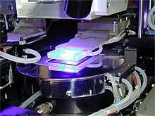
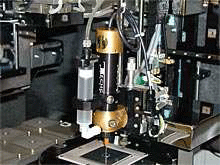
FC300: The High Force and High Accuracy Die Bonder for Large Devices The tool features automated handling of chips and substrates up to 100 mm from waffle packs, plus a robotic option enabling chip picking from diced wafer and automated handling of larger substrate. It features also Nanoimprinting Lithography (NIL) capabilities. With a quick process head reconfiguration, the FC300 platform performs multiple applications including: * High Force, particularly interesting for Cu-Cu bonding as used in 3D-IC packaging, or Nanoimprinting using a Hot Embossing Lithography process;
* Low Force Reflow Bonding for imaging devices, RF, or Optoelectronics assembly;
* UV-Curing for a Adhesive Bonding or for Nanoimprinting using a UV-NIL process.
* Its ± .5 micron post-bonding accuracy and
20 micro-radians leveling guarantee high yields on the most advanced products * Semi-Open Confinement Chamber for Oxide Reduction option
* Bonding of devices up to 100 x 100 mm onto wafer up to 300 mm to
enable large format assemblies
* NIL configuration as add-on to bonding capability for maximum flexibility
* Optional Gas Confinement Chamber with inert or reducing gas for in-situ removal of oxides during bonding
* Air bearing construction on a granite structure ensures
long-term stability and reliability * Optional integrated chamber for gang reflow in a gas or vacuum environment
High End Processes Die Bonding (Face Up), Flip Chip Bonding (Face to Face), Mass Reflow, In-Situ Reflow, Fluxless Eutectic Bonding, Thermocompression Bonding, Ultrasonic Bonding, UV-Curing Bonding, Adhesive Bonding, UV-NIL, Hot Embossing Lithography...
.
FC150 Automated Device Bonder Originally developed in 1981 through collaboration with CEA/LETI to answer infrared detection needs, the FC150 Automated Device Bonder offers the latest evolution in bonding techniques. Available as a completely automated system to level, align and package components ranging from 200 Fm up to 100 mm, the FC150 supports the complete range of bonding applications including optoelectronics and MEMS. With configurations ranging from manual to full automation, the FC150 provides development and production capabilities on a single cost-effective platform.
* Its ± 1 micrometer 3 sigma post-bonding accuracy and
20 micro-radians levelling guarantee high yields on the most advanced products * Air bearing construction on a granite structure ensures
long-term stability and reliability * Compression or gap control, and temperature profiling
on both upper and lower components, together with process monitoring, maximize process control * Optional automatic levelling and alignment allow
hands-off operation for production applications
. |
JB Technical Support Service, LLC.
|
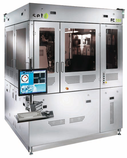 Features and Benefits
 />
/>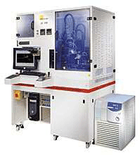 Features and Benefits